| Email not displaying correctly? View it in your browser. |
 Volume 2 Issue 3 - March 2009
 |
|
The NNN Newsletter
Economic Impact of Nanomanufacturing Initiatives
Early projections for global market growth of nano-enabled products—which have increased by about 25% per year since 2000 and predict US $1 trillion by 2015—are still relevant in 2009. With significant investment for nanoscience and technology initiatives being seeded at the federal and state levels, new models have emerged for sustaining critical research within academic institutions while providing the necessary industrial interactions to transition key technologies for commercialization. A growing trend for new initiatives around the U.S. includes regional, state, and local collaboration in nanoscience research and development. Such initiatives target critical research and development partnerships for sustainable commercialization of nano-enabled products. Regional efforts are typically established around core academic research institutions providing an integral industrial partnering platform for R&D, technology transfer, and commercial scale-up. The technology focus may be based on key expertise of the institution and target specific industrial sectors. While most states have embraced this model in order to attract and sustain a new industrial base, the economic impact is not always immediately evident, and may take years to emerge. Impact and success will ultimately depend on multiple factors including size of the industrial sector being targeted, initial funding by state and federal sources, industry matching funds, strategies for licensing, commercialization, and economic growth. Regards,
|
Upcoming Events March 23, 2009 March 26, 2009 March 29 - April 2, 2009 April 1 - 2, 2009 April 1 - 3, 2009
Advertisement
Advertisement Affiliated Centers
Recently Published Vapor-Phase Formation of Alkyl Isocyanate-Derived Self-Assembled Monolayers on Titanium Dioxide Linear Dipole Behavior in Single CdSe-Oligo (phenylene-vinylene)
Nanostructures
Directed Assembly of Polymer Blends Using Nanopatterned Templates Centrifugal Sedimentation for Selectively Packing Channels with Silica Microbeads in Three Dimensional-Micro/Nanofluidic Devices |
|
The National Nanomanufacturing Network Newsletter Subscribe / Unsubscribe from this list. Our mailing address is: The National Nanomanufacturing Network 322 Lederle Graduate Research Center 710 N. Pleasant Street University of Massachusetts Amherst, MA 01003 Our email address is: nnn@nanomanufacturing.org Our phone number is: (413) 577-0570 Copyright (C) 2008 The National Nanomanufacturing Network All rights reserved. Supported by the National Science Foundation under Grant No. DMI-0531171. |
|

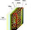 While
single-crystal silicon based photovoltaics are a well-developed
technology, the costs associated with producing and fabricating
high-purity Si limit the widespread use of photovoltaics as a renewable
energy source. Recent efforts to circumvent these costs have focused
on a number of developing technologies, including polymer- and nanomaterial-based
solar cells. A recent paper by Kortshagen and co-workers reports
a photovoltaic cell with a photoactive region consisting of a blend
of Si nanocrystals and conductive polymer P3HT that can be processed
from solution. The solution processability of this �hybrid� solar
cell is ideally suited for inexpensive, large-scale manufacture,
while the use of Si nanocrystals avoids the presence of heavy metals.
While
single-crystal silicon based photovoltaics are a well-developed
technology, the costs associated with producing and fabricating
high-purity Si limit the widespread use of photovoltaics as a renewable
energy source. Recent efforts to circumvent these costs have focused
on a number of developing technologies, including polymer- and nanomaterial-based
solar cells. A recent paper by Kortshagen and co-workers reports
a photovoltaic cell with a photoactive region consisting of a blend
of Si nanocrystals and conductive polymer P3HT that can be processed
from solution. The solution processability of this �hybrid� solar
cell is ideally suited for inexpensive, large-scale manufacture,
while the use of Si nanocrystals avoids the presence of heavy metals.
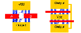 The interest in developing electronic devices based on single-wall carbon nanotubes (SWNT) derives from the promise of higher performance than silicon-based CMOS integrated circuits, which are at the heart of the microelectronics industry. Among the challenges to fabricate SWNT devices at a wafer-scale are the difficulty of synthetizing carbon nanotubes with controlled chirality and therefore controlled transport properties and the accurate positioning and electrical addressing of a large number of nanotubes. The idea at the core of Ryu and colleagues' recently-published report is the use of a horizontal array of aligned, non-overlapping nanotubes with lithographically patterned electrical contacts for a group of nanotubes. This paper describes advances obtained in multiple fabrication steps, which enable the implementation of advanced electronic logic functions at a full 4� wafer scale.
 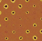 Compared to conventional lithographic methods for the preparation of nanostructures, which typically reqire time-consuming process sequences and expensive masks, Laser Interference Lithography (LIL) is an inexpensive and efficient option to produce nanopatterns over large areas. An international team of researchers demonstrates a simplified method of laser interference lithography for ordered surface nanostructures <5nm.