|
The NNN Newsletter
NIST TIP Invests
in Nanomanufacturing
 The U.S. Commerce Department’s National Institute of Standards and Technology (NIST) announced in December 2009 over $31 million in funding through its Technology Innovation Program (TIP) for nine new cost-sharing projects that will support innovative, high-risk research in novel nanomaterials or nanomanufacturing technologies that address critical national needs. TIP is focused on developing new materials based on nanotechnology—advanced composites and “superalloys,” or smart materials—and expanding the capacity to incorporate these materials into new products. The acceleration of advanced nanomaterials and nanomanufacturing is a critical strategy to advance the growth and competitiveness of U.S. manufacturing. Several key issues of nanomaterials production and nanomanufacturing were specifically cited in the NIST white paper; "Accelerating the Incorporation of Materials Advances into Manufacturing Processes." The U.S. Commerce Department’s National Institute of Standards and Technology (NIST) announced in December 2009 over $31 million in funding through its Technology Innovation Program (TIP) for nine new cost-sharing projects that will support innovative, high-risk research in novel nanomaterials or nanomanufacturing technologies that address critical national needs. TIP is focused on developing new materials based on nanotechnology—advanced composites and “superalloys,” or smart materials—and expanding the capacity to incorporate these materials into new products. The acceleration of advanced nanomaterials and nanomanufacturing is a critical strategy to advance the growth and competitiveness of U.S. manufacturing. Several key issues of nanomaterials production and nanomanufacturing were specifically cited in the NIST white paper; "Accelerating the Incorporation of Materials Advances into Manufacturing Processes."
While the new projects funded by NIST TIP included research for sensing and repair materials for infrastructure (bridges, water, dams, roads, etc.), specific projects advancing nanomaterials and nanomanufacturing garnered almost half of the total funding. These projects include advanced electrode materials and scaled manufacturing for batteries, scaled volume production of nanomaterials, including carbon nanotubes, graphene, carbon nanofibers, and composite nanoparticles.
More...
Regards,
Jeff Morse, Managing Director,
National Nanomanufacturing Network
Learn More about the 
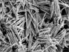
Metal-Catalyst-Free CVD Synthesis of Carbon Nanotubes
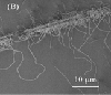 Until a few years ago, it was believed that CVD synthesis of single wall carbon nanotubes (SWNT) should incorporate transition metal nanoparticles, such as Fe, Ni, and Co, as catalysts. However, recent investigations on SWNT CVD are expanding this range of catalyst materials toward non-transition metals, noble metals, and most promisingly toward non-metallic materials. CNT growth on non-metallic nanostructures can facilitate application of the CNT materials to semiconductor technology, pharmaceutical technology, membrane technology and basic sciences. Metal-free SWNT will remove a detrimental incompatibility issue in semiconductor electronics fabrication (CMOS) process that has not allowed adaptation of CNTs, as-synthesized or transplanted, onto an electronics substrate because of the contamination issues associated with metal catalyst particles. Metal-catalyst-free CNTs would enable much easier purification, mitigate a toxicity concerns, and lower the price of pure CNT materials, which may further extend the scope of these material applications. Membrane- or CNT-Nanofluidics-based research and industry could also benefit from the metal-free CNT in order to bypass one or more manufacturing steps, leading toward cost-effectiveness. More.... Until a few years ago, it was believed that CVD synthesis of single wall carbon nanotubes (SWNT) should incorporate transition metal nanoparticles, such as Fe, Ni, and Co, as catalysts. However, recent investigations on SWNT CVD are expanding this range of catalyst materials toward non-transition metals, noble metals, and most promisingly toward non-metallic materials. CNT growth on non-metallic nanostructures can facilitate application of the CNT materials to semiconductor technology, pharmaceutical technology, membrane technology and basic sciences. Metal-free SWNT will remove a detrimental incompatibility issue in semiconductor electronics fabrication (CMOS) process that has not allowed adaptation of CNTs, as-synthesized or transplanted, onto an electronics substrate because of the contamination issues associated with metal catalyst particles. Metal-catalyst-free CNTs would enable much easier purification, mitigate a toxicity concerns, and lower the price of pure CNT materials, which may further extend the scope of these material applications. Membrane- or CNT-Nanofluidics-based research and industry could also benefit from the metal-free CNT in order to bypass one or more manufacturing steps, leading toward cost-effectiveness. More....
|
Directed Self Assembly
This
article is the first in a series of briefs on the directed
self assembly of nanostructures.
 Deterministic Field Assisted Assembly Deterministic Field Assisted Assembly
by Theresa S. Mayer, Pennsylvania State University
Traditional chip fabrication relies on multilevel photolithography to define device features. It gives excellent control of feature geometry and registration over different levels, but places considerable limits on the materials and molecules that can be incorporated. Alternatively, nanocomponents can be synthesized prior to assembly onto the chip, providing much greater diversity in materials often at the expense of accurate placement. The deterministic field assisted assembly integration strategy solves this problem by using electric field forces to direct different components to specific regions of the chip, while providing accurate registry between each individual part and the lithographic features in that region. This allows us to add entirely new capabilities on top of the existing powerful, inexpensive processing and storage functions of silicon. More....
|
Nanotechnology Prevalent Among 2009 R&D 100 Competition Winners
 Nanotechnology was a common theme contributing to many of last year’s R&D 100 competition winners. The competition, sponsored by R&D Magazine, considers technologies transitioning from research laboratories to commercialization, and selects winning submissions based on several figures of merit including intellectual innovation, market application, and technical maturity. This years winners included a range of micro and nanotechnologies covering a range of categories such as energy and power, electronics, microscopy, analytical instruments, nanomaterials, processes, and nanomanufacturing. While many were specific nanotechnologies, others were enabled through incorporation of nanoscopic elements. Examples of this year’s field of competition are described below, and additional information can be found at R&D Magazine. More... Nanotechnology was a common theme contributing to many of last year’s R&D 100 competition winners. The competition, sponsored by R&D Magazine, considers technologies transitioning from research laboratories to commercialization, and selects winning submissions based on several figures of merit including intellectual innovation, market application, and technical maturity. This years winners included a range of micro and nanotechnologies covering a range of categories such as energy and power, electronics, microscopy, analytical instruments, nanomaterials, processes, and nanomanufacturing. While many were specific nanotechnologies, others were enabled through incorporation of nanoscopic elements. Examples of this year’s field of competition are described below, and additional information can be found at R&D Magazine. More...
Read more on 
|
Upcoming Events
February 2, 2010
CHN Industry Showcase
February 3 - 4, 2010
4th Tri-National Workshop on Standards for Nanotechnology
February 9, 2010
Understanding Nanomanufacturing
February 14 - 18, 2010
TMS 2010 Annual Meeting & Exhibition
February 21 - 25, 2010
SPIE Advanced Lithography
Advertisement

Upcoming Calls
January 29, 2010
Nanosens 2010
Deadline to submit abstracts
January 31, 2010
Particles 2010
Deadline to submit abstracts
February 1, 2010
Nanomanufacturing Conference and Exhibits
Deadline to submit poster abstracts
February 26, 2010
ANGEL 2010
Deadline to submit abstracts
March 19, 2010
Nanotoxicology 2010
Deadline to submit abstracts
Advertisement
Recently Published
From Our Affiliates
Analytical and Experimental Studies of the Mechanics of Deformation in
a Solid With a Wavy Surface Profile
Journal of Applied Mechanics 77(1): 011003
2,3-Bis(bromomethyl)-1,4-diphenylbenzene
Acta Crystallographica Section E Structure Reports Online 66(Part 1)
Advertisement

Affiliated Centers


Advertisement


|
 Volume
3 Issue 1 - January 2010
Volume
3 Issue 1 - January 2010