Deterministic Field Assisted Assembly
by Theresa S. Mayer and Christine D. Keating, Pennsylvania State University
Silicon electronics could be made to run cooler or to interact with the environment by adding new materials and devices atop the circuitry. Attractive new materials include narrow bandgap semiconductors that operate at lower voltages than silicon, giving lower power consumption without sacrificing speed. Molecular and metal oxide materials, which can produce a large electronic response to chemical vapors or biological molecules, offer sensing capabilities. Unfortunately, the high temperatures and harsh chemicals used in conventional fabrication processes generally destroy these materials or the chips themselves, which up to now has made it impossible to effectively couple them.

Unique Aspects
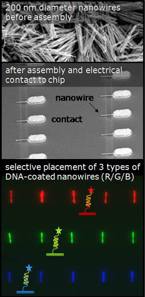
Traditional chip fabrication relies on multilevel photolithography to define device features. It gives excellent control of feature geometry and registration over different levels, but places considerable limits on the materials and molecules that can be incorporated. Alternatively, nanocomponents can be synthesized prior to assembly onto the chip, providing much greater diversity in materials often at the expense of accurate placement. The deterministic field assisted assembly integration strategy solves this problem by using electric field forces to direct different components to specific regions of the chip, while providing accurate registry between each individual part and the lithographic features in that region. This allows us to add entirely new capabilities on top of the existing powerful, inexpensive processing and storage functions of silicon.
Relevance
The International Technology Roadmap for Semiconductors (ITRS) highlights not only the need to continue silicon CMOS miniaturization, but also the growing importance of expanding its capabilities by adding new materials and devices. The seamless integration of power sources, RF communication, sensors, actuators, and biological functions will allow future chips to interact directly with people and the environment. However, inherent incompatibilities between the CMOS circuit and nanomaterial fabrication conditions must first be overcome. Deterministic field assisted assembly meets this challenge using the powerful concept of programmed assembly, which can be generalized to connect almost any nanomaterial component directly to the transistor circuitry on the chip. Off-chip component fabrication allows the luxury of optimizing process conditions for a given material (temperatures, chemicals, mixing, etc.), while still employing conventional methods to build the electronic circuitry.
Current Efforts
This new nanofabrication technology that has the potential to add new materials and devices after silicon chips are made. Our recent breakthroughs in programmed nanomaterial assembly have shown that this is possible. We have directed different populations of DNA-coated nanowires to specific regions of the chip with the submicron placement accuracy that enables fabrication of electrical connections between individual nanowires and specific transistors on the chip. Individual nanowire assembly yields of greater than 80% were achieved for arrays containing several thousand nanowires integrated at densities exceeding 106/cm2. The experiments confirmed the retention of binding selectivity for the probe DNA on the assembled nanowires despite exposure to electric fields, photoresist coatings, and solvents.
We have also fabricated active devices from diverse nanomaterials including semiconductor, conducting polymer, and metal nanowires. Notably, the performance of cantilevered semiconductor resonators, polythiophene nanowire chemical sensors, and axially-doped silicon nanowire field effect transistors matched or exceeded similar stand alone devices fabricated by conventional methods.
References
This work is licensed under a Creative Commons Attribution-NonCommercial 3.0 Unported.
