| Directed self-assembly (DSA) of nanoscale devices commonly combines self-assembling materials such as block copolymers (BCPs) with lithographically defined pre-patterned surfaces. To date, the most significant impact of DSA has been for the fabrication of nanoimprint master molds for bit-patterned magnetic storage media. Moving to semiconductor integrated circuit fabrication requires DSA strategies that adhere to the stringent requirements for wafer-scale integration and compatibility with semiconductor process techniques. Cheng et. al. demonstrate a straightforward approach to integrate DSA with either chemical or topographical pre-patterns using optical lithography and conventional 193 nm photoresists. |
Reviewed by Jeff Morse, PhD, National Nanomanufacturing Network
Directed self-assembly (DSA) of nanoscale devices commonly combines self-assembling materials such as block copolymers (BCPs) with lithographically defined pre-patterned surfaces. As such, the lithographically defined pre-patterns—either topographically or chemically modified features over a surface—effectively guide the assembly of sub-lithographic resolution patterns, which can then be used as masks for subsequent process steps. To date, the most significant impact of DSA has been for the fabrication of nanoimprint master molds for bit-patterned magnetic storage media. Utilizing electron beam direct write or ultraviolet interference lithography to create the initial nanoscale features, pattern frequency multiplication is achieved with appropriate self-assembling materials. For applications in bit-patterned media, the process requirements are somewhat relaxed as the pattern only needs to be achieved once to create the initial master template. In comparison, semiconductor integrated circuit fabrication requires DSA strategies that adhere to the stringent requirements for wafer scale integration including low defectivity, low cost, short cycle time, and compatibility with semiconductor process techniques.
A key step in addressing these challenges is to integrate DSA with commercial optical lithography in order to evaluate and compare various parameters and metrics for the approach, including resolution, line-edge roughness, overlay, and defectivity. In the case of 193 nm water immersion lithography, the practical resolution limit of 40 nm half-pitch has been achieved. In order to utilize the patterning capabilities of present optical lithography until next generation technologies are available, techniques such as self-aligned double patterning (SADP) are being explored, which doubles the spatial frequency of the photoresist pattern. While this method has gained acceptance, the stringent process control requirements and growing development costs represent a roadblock for using sequential SADP for higher-order pattern frequency multiplication. This is where DSA could provide a more efficient pattern multiplication approach and extend present optical lithography beyond double patterning. However, typical DSA processes utilize organic casting solvents and high temperature anneal steps that will degrade the fidelity of typical photoresist pre-patterns. Some DSA approaches have been explored where the patterned photoresist is used as a sacrificial layer to transfer a robust topographical or chemical pre-pattern onto an underlying hardmask material, although this requires additional process steps and added cost.

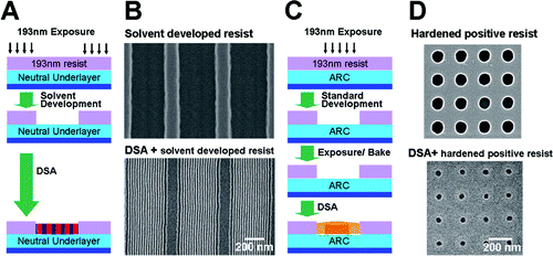
Recently, Cheng et. al. investigated an approach to integrate DSA with either chemical or topographical pre-patterns using optical lithography and conventional 193 nm photoresists. In this study, the authors found that polarity-switched, chemically amplified photoresist materials exhibited increased thermal stability as well as insolubility to solvents used in the casting of self-assembling materials systems. In order to achieve an effective pitch division splitting pre-patterning process for DSA, it is important to control the surface chemistry of the top surface, sidewalls, and bottom recessed surface of the guiding features in order to achieve the desired morphology of the self-assembled patterns. In part, it is critical to maintain a neutral underlying surface with respect to affinity towards one of the BCP domains in order to achieve vertically aligned structures.
To bypass this issue, the authors demonstrated negative tone development using a standard positive tone resist by switching from the usual tetramethylammonium hydroxide (TMAH) aqueous developer to an organic solvent such as anisole. In this case, the exposed regions become polar de-protected and remain insoluble, thus the patterned surface chemistry can be better controlled for subsequent casting of self-assembling materials. The polarity-switched photoresist material exhibits excellent hardened properties (i.e; it is not soluble in many organic solvents and can withstand high temperature anneal steps). Furthermore, the polarity-switching process renders the material rich with carboxylic acid, therefore retaining an affinity for the more polar block of a BCP blend. In this manner the polarity-switched photoresist helps to align the BCP domains parallel to the pre-pattern template. Using this approach, the authors were able to form 370 nm trench patterns. A polystyrene-b-polymethyl methacrylate (PS-b-PMMA) diblock copolymer was spun cast on the photoresist pre-pattern. With the affinity of the PMMA for the resist sidewall and the neutrality of the underlayer at the bottom of the trenches, the BCP domains formed parallel to the trench with vertical orientation. The resulting domains were 24.8 nm in width.
The authors further demonstrated DSA using chemical pre-patterns with conventional positive tone photoresists. In this approach, positive tone patterns are formed by mask exposure and development in TMAH, which alters the surface chemistry of the underlayer. Next, a neutralizing film is deposited over the entire surface. The entire substrate is then flood exposed, followed by a liftoff using TMAH to remove any remaining photoresist and leave a chemically altered surface that effectively guides the DSA patterns. Subsequent casting of PS-b-PMMA and thermal annealing resulted in frequency quadrupled BCP domain patterns critical dimensions on the order of 13 nm.
A straightforward method to integrate DSA with optical lithography has been demonstrated. The approach described requires no added processing complexity for 193 nm immersion lithography. The approach is further compatible with conventional lithographic processes and cycle times, and can subsequently be performed in fully automated wafer track tools. Additionally, the same general principles apply to a wider range of chemically amplified photoresists, and can thereby enable the integration of DSA with a range of optical lithography tools.
Image reproduced with permission from Cheng JY, et al. 2010. Simple and Versatile Methods to Integrate Directed Self-Assembly with Optical Lithography Using a Polarity-Switched Photoresist. ACS Nano Article ASAP July 15, 2010. DOI: 10.1021/nn100686v. Copyright American Chemical Society 2010.
This work is licensed under a Creative Commons Attribution-NonCommercial 3.0 Unported.
