
| Synthesis of nanoporous structures utilizing more traditional fabrication routes typically incorporate lithographic patterning, followed by a wet or plasma etch step. Yet these processes are expensive and introduce complicating issues such as the infiltration of resist or thermoplastic materials within the pore network, which may alter the structure and is difficult to remove, as well as the challenge of retaining pattern fidelity during the etch step. For rapid, low-cost, large-area fabrication of patterned features and structures in nanoporous media, a facile, reproducible, direct printing process is required. Recently, Ryckman et. al. describe such a rapid, low-cost approach for patterning porous nanomaterials using a direct imprinting process that enables the capability to form complex networks and structures for a range of potential applications. |
Reviewed by Jeff Morse, PhD., National Nanomanufacturing Network
Porous nanomaterials have been investigated for many years for a wide range of applications from drug delivery, chemical and biological sensors, and catalysis to solar photovoltaics, battery electrodes, integrated optoelectronics, and plasmonics. These materials are characterized as nanostructured void networks with high specific surface areas providing unique optical, electrical, chemical, and mechanical properties. Example materials include porous silicon (pSi), porous alumina (pAl2O3), nanoporous gold (np-Au), and titania nanotube arrays (TiO2-NTA). In these cases, the porous nanomaterial formation is achieved via facile, self-organizing processes. In order to extend the application of such materials, it is desirable to form micro and macroscale structures from which more complex device concepts can be realized.
Synthesis of such structures utilizing more traditional fabrication routes would typically incorporate lithographic patterning, followed by a wet or plasma etch step. Yet these processes are expensive and introduce additional issues such as the infiltration of resist or thermoplastic materials within the pore network, which may alter the structure and is difficult to remove, as well as the challenge of retaining pattern fidelity during the etch step. For rapid, low-cost, large-area fabrication of patterned features and structures in nanoporous media, a facile, reproducible, direct printing process is required.
Recently, Ryckman et. al. reported on the investigation of a rapid, low-cost approach for patterning porous nanomaterials using a direct imprinting process. The concept behind this research is that material containing a heterogeneous network of voids can accommodate a volume change approaching the total void fraction. Utilizing a pre-patterned stamp, similar to nanoimprint lithography patterning, the porous nanomaterial is selectively compressed by the stamp pattern. The compression effectively crushes the porous material while leaving the uncompressed material in tact. Using a master pattern formed in a silicon wafer by photolithographic patterning and reactive ion etching, the authors demonstrated the direct imprinting of porous substrates (DIPS) process on a range of porous nanomaterials including those mentioned above.
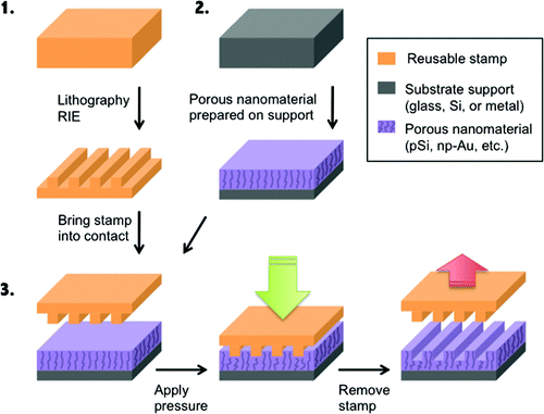
To extend the versatility of the DIPS method, the authors further demonstrated that a second stamping step could be conducted to form even more complex networks of nanoporous materials structures. Furthermore, an intermediate etch step can be conducted to change the porosity between the original material pattern and the subsequent stamping step in order to enable additional complexity to the resulting porous network structure. Furthermore, scanning electron micrograph (SEM) imaging of the stamped patterns exhibited excellent fidelity in the patterns formed in the porous materials structures studied. Finally, for achieving high aspect ratio structures, the theoretical limit for the stamping process is the fraction of voids present in the porous material structures. As an example, the authors patterned grating structures in a 1 µm thick, 80% by volume pSi film. The resulting patterns were ~780 nm deep, very close to the theoretical limit for this particular film.
Thus a versatile, simple approach has been reported for patterning structures with nanoporous materials enabling the capability to form more complex networks and structures for a range of potential applications. Furthermore, while the initial studies were conducted on fairly small samples, additional demonstration of this at the wafer scale and beyond has the potential for a significant impact on technologies utilizing nanoporous materials structures.
Image reproduced with permission from Ryckman JD, et. al., Nano Letters Article ASAP 17 September 2010. DOI: 10.1021/nl1028073. Copyright 2010 American Chemical Society.