Inkjet printing is a promising technique for printing of electronic materials and devices over large areas on flexible substrates. Inkjet printing is a versatile approach involving a limited number of steps with the ability to deposit controlled amounts of material. The development of inks for inkjet printing can be tailored to optimize the properties of the printed films and structures, and are additionally versatile in that virtually any nanomaterial composition can be incorporated as long as the nanostructure size is sufficiently small that the inkjet nozzle does not become clogged. The rule of thumb is nanostructure feature sizes ~1/50 the diameter of the nozzle. Solution dispersed nanostructures are being investigated as a means to incorporate semiconducting materials in printed thin films for electronic structures and devices. In the case of printed thin-film transistors (TFTs), the charge carrier mobility is much lower than that possible using crystalline silicon, typically on the order of 0.1-1.0 cm2/V-sec. One way to increase the carrier mobility of solution based printed TFTs is to utilize nanostructured materials having superior electronic transport properties, such as graphene or carbon nanotubes. The process described below describes the ink formulation and method for inkjet printed graphene films having charge carrier mobility up to 50 cm2/V-sec. Liquid phase exfoliation (LPE) is ideally suited to produce printable inks. LPE was achieved through sonication of graphite oxide following the Hummers method. By dispersing the graphene in N-Methyl-2-pyrrolidone (NMP) and using low power ultrasonication steps, the electronic properties of the graphene nanostructures are preserved by introducing less defects. Furthermore, the use of NMP provides a means to optimize the properties of of the ink for the inkjet deposition parameters.
Felice Torrisi, Tawfique Hasan, Weiping Wu, Zhipei Sun, Antonio Lombardo, Tero S. Kulmala, Gen-Wen Hsieh, Sungjune Jung, Francesco Bonaccorso, Philip J. Paul, Daping Chu, and Andrea C. Ferrari
Department of Engineering, Cambridge Graphene Centre


Graphite flakes (NGS Naturgraphit) are ultrasonicated (Decon bath, 20W) in NMP for 9 h. The unexfoliated flakes are left to settle for 10 min after ultrasonically
The decanted dispersion are then ultracentrifuged using a TH-641 swinging bucket rotor in a Sorvall WX-100 ultracentrifuge at 10000 rpm for 1 hour, then filtered to remove flakes >1 µm that might clog the nozzle.
The resulting dispersion has the following properties:
Viscosity: ~1.9 mPa s
Surface Tension: ~40 mJ m<sup>-2</sup>
Density: 1.05 gcm<sup>-3</sup>
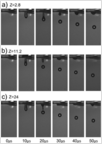
In order to adjust the dimensionless parameter Z within the optimal range for drop on demand printing, the above parameters were modified by mixing the ink with additional exfoliated graphene (EG).
20% EG/80% Graphene Ink: Z=11.2
80% EG/20% Graphene Ink: Z=2.8
Nominal: 1
Inkjet Printing: Epson Stylus 1500 inkjet printer with a S020049 cartridge under a constant nitrogen flow.
Substrate: Silicon dioxide passivated silicon
Surface Preparation:Adjust substrate surface energy to control ink droplet spreading.
a. pristine
b. Hexamethyldisilazane (HMDS)-coated: HMDS is deposited by spin coating for 40 s at 1000 rpm, followed by annealing at 80 C for 2 min.
c. O<sub>2</sub>-plasma-treated Si/SiO<sub>2</sub>: the O<sub>2</sub> plasma is generated at 200 W and 4x10<sup>-1</sup> Torr for 2 min.
Variation of surface energy on which ink is printed will control properties of printed pattern.
- TH-641 swinging bucket rotor
- optical absorption spectroscopy
- high-resolution transmission electron microscopy
- electron diffraction
- Raman spectroscopy
- Epson Stylus 1500 inkjet printer with a S020049 cartridge under a constant nitrogen flow.
