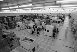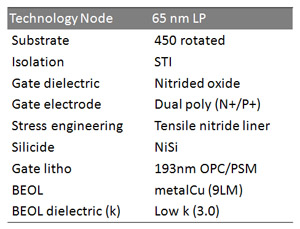
Currently, the main cleanroom (see Figure 1) is populated with a complete tool set capable of developing both CMOS technologies with feature sizes of 15nm and low-volume early-user hardware production at more mature technology nodes (e.g., 65nm). Our lithography tool set features production-grade equipment, including immersion single-pass (ASML 1700i), immersion double-patterning (ASML 1950i), extreme-UV (EUV), e-beam, and imprint lithography. CNSE features an ASML Alpha Demo Tool (ADT). A future expansion that will include manufacturing-grade EUV tools is under consideration. This will take the college's production-worthy lithography capability beyond the 15nm node.

Unique opportunities exist to develop process features that require introduction of novel materials, a typically difficult challenge in more traditional manufacturing environments. While CNSE follows industry-standard procedures for contamination control, the facility's research and development nature lends itself to explore integration of unique process elements involving materials not proven compatible with standard CMOS, such as resistive random-access memory or spin-based memory elements. For example, and part of an ongoing, more future-oriented research project, CNSE is introducing graphene into the cleanroom, which involves addressing contamination-control issues because of the nature of the catalytic-growth conditions used to grow graphene.
In 2010, the college is expanding its facilities and partners to build a packaging center on campus that will initially focus on development of 300mm wafer-scale 3D integration. This capability allows heterogeneous integration of micro-electromechanical systems (MEMS) sensors, optical components, and RF applications.

The 0.3NA (numerical aperture) Albany Exitech micro-exposure tool (eMET) and the 0.25NA ADT provide imaging support to joint development and research partners. The eMET is ideally suited for contrast-curve generation and was developed as a screening tool to allow resist manufacturers to do coarse screening of large quantities of samples. Today, the eMET can easily accomplish a coarse screen of five or more samples, allowing testing of the best candidates for maximum resolution on the Lawrence Berkeley National Laboratory micro-exposure tool. This system is capable of imaging in the 22nm range and below.
CSNE has developed and built a state-of-the-art outgassing test stand. With this equipment, resists and materials are qualified before use on the EUV exposure systems.1,2 Once the best candidates in terms of resolution, linewidth roughness (LWR), and photospeed have been identified, the materials are typically tested on the full-field ADT. CNSE and SEMATECH staff handle all imaging and wafer processing and may also analyze and provide the data to facility users. A typical user will receive outgassing results, contrast-curve information, process-window data, ultimate resolution, critical-dimension uniformity, and LWR.
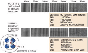
So far this year, more than 2000 wafers have been exposed on the eMET tool. The eMET is delivering 90% availability (24 hours, 7 days a week). This performance has allowed characterization of hundreds of resist and underlayer samples. The eMET can now image 24nm routinely and shows modulation at 22nm (see Figure 2). Future planned upgrades will drive resolution to sub-20nm levels.
References
- G. Denbeaux, Extreme ultraviolet resist outgassing and its effect on nearby optics, Proc. SPIE 6921, pp. 69211G, 2008. doi:10.1117/12.772670
- G. Denbeaux, Quantitative measurement of EUV resist outgassing, Proc. SPIE 6533, pp. 653318, 2007. doi:10.1117/12.737192
This article was originally published in the SPIE Newsroom.
