Indium arsenide (InAs) nanowires (NWs) have gained wide interest due to high carrier mobility and quantum confinement properties, making them excellent candidates for high-speed and high-frequency electronic devices. A drawback of InAs remains the narrow electronic bandgap, which results in excessive leakage currents for subsequent device applications. Approaches to resolving this have investigated complicated materials systems such as indium phosphide heterojunctions (InAs/InP) or segments of InAsP along the InAs-NW length. Indium gallium arsenide (InGaAs) is one potential material system that can be grown through continuous processes while controlling the electronic bandgap and mobility through composition. Growth of In-rich NWs still retains the superior electronic properties of InAs while reducing the leakage current.
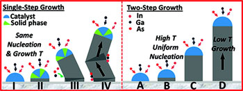
SEM and (inset) TEM images of NWs grown by the two-step method (growth condition: source temperature at 800 °C, substrate temperature at 540 °C, H2 flow rate at 100 sccm, growth duration of first step is 1 min and second step is 30 min); the scale bars are 2 ¼m and 200 nm, respectively.The growth of InGaAs is typically achieved using a high temperature catalytic solid-source chemical vapor deposition (CVD) method. Using gold (Au) as the catalyst, Au nanoparticles are formed by thermal annealing a 0.5 nm film of gold coated on an oxidized silicon substrate at ~800°C, followed by NW growth as the precursor vapors are supplied from the heated solid source. Growth of InGaAs nanowires is plagued by defect and morphology issues during single step growth due to the similarity in temperatures between the catalyst anneal and the NW growth steps. As a result, the catalyst nanoparticle experiences a liquid-solid phase interface that leads to inhomogeneous NW growth, and a kinked NW morphology indicative of significant defects within the NW structures. Recently, Hou et. al. investigated a two-step growth process wherein the catalyst anneal was conducted at a high temperature, then the source and substrate zones were cooled to better control the reactant delivery and growth conditions of the NWs. The added nucleation step prior to growth significantly reduced the kinked morphology, defect density, and previously observed surface coatings that formed around the NWs. The lower temperature growth conditions provide a more favorable mechanism resulting in straighter NWs having smoother surface. The mechanism is facilitated by eliminating the formation of a solid phase at the catalyst interface, thereby enabling uniform, preferential growth of NWs following the well-established vapor-liquid-solid (VLS) growth process.
(a) (Top) SEM and (bottom) schematic of a back-gated InGaAs NW array FET. The scale bar is 1 ¼m. The designated channel length and width are 2 and 200 ¼m, respectively. (b) Transfer characteristic of a representative InGaAs NW parallel device under VDS = 0.1, 0.4, 0.7, and 1 V, about 200 NWs bridging S/D. Characterization of the In-rich InGaAs NWs verified the high crystalline quality produced by the two-step growth process, with typical NWs having ~10 µm length and 30 nm diameter. Growth densities were >5 NWs/µm2 under optimized conditions. Field effect transistors (FETs) were fabricated from individual and arrays of the InGaAs NWs. Utilizing a oxidized conductive silicon substrate in a back gate FET design, nickel source-drain electrodes were patterned with a gate length of ~2 µm. Characterization of the single NW device demonstrated ION/IOFF ratios of ~105, with estimated carrier mobility of ~2700 cm2/V-sec. The single NW FET further demonstrated a current density of 0.9 mA/µm, comparable to state-of-the-art silicon MOSFETS. Contact printing was used to fabricate a large scale integrated FET design with 200 NWs patterned in a gate structure having length ~2 µm and width of 200µm. The resulting properties for the scaled device were not quite as impressive, with ION/IOFF ratios of ~500, with estimated carrier mobility of ~60 cm2/V-sec, which is comparable to reported devices fabricated from carbon nanotube networks. Thus a two-step growth process has been reported, which is capable of producing high quality InGaAs NWs. The growth process exhibits a wide process window, thereby enabling reproducible growth of precisely tailored In-rich InGaAs NWs for electronic devices. While FET devices fabricated from a single NW exhibited impressive performance properties, array based FET devices were not able to maintain the properties of the individual NW elements, one of the key challenges in nanomanufacturing. Further investigation of the cause of this scaling limitation will enable improved understanding of semiconductor NWs for scaled electronic device integration.
Reviewed by Jeff Morse, PhD, National Nanomanufacturing Network
Hou JJ, Han N, Wang F, Xiu F, Yip SP, Hui AT, Hung TF, Ho JC. 2012. Synthesis and characterizations of ternary InGaAs nanowires by a two-step growth method for high-performance electronic devices. ACS Nano. Article ASAP. http://dx.doi.org/10.1021/nn300966j
Figures reprinted with permission from Hou JJ, Han N, Wang F, Xiu F, Yip SP, Hui AT, Hung TF, Ho JC. 2012. Synthesis and characterizations of ternary InGaAs nanowires by a two-step growth method for high-performance electronic devices. ACS Nano. Article ASAP. http://dx.doi.org/10.1021/nn300966j

 TEM images of NWs grown by the two-step method (growth condition: source temperature at 800 °C, substrate temperature at 540 °C, H2 flow rate at 100 sccm, growth duration of first step is 1 min and second step is 30 min); the scale bars are 2 ¼m and 200 nm, respectively.")
 (Top) SEM and (bottom) schematic of a back-gated InGaAs NW array FET. The scale bar is 1 ¼m. The designated channel length and width are 2 and 200 ¼m, respectively. (b) Transfer characteristic of a representative InGaAs NW parallel device under VDS = 0.1, 0.4, 0.7, and 1 V, about 200 NWs bridging S/D.")