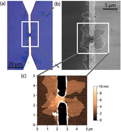
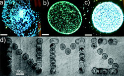
Nanomanufacturing processes are typically unique methods employed to control the shape, features, size, and morphology of materials in order to achieve some value-added functionality. Depending on the targeted objectives, numerous approaches and materials could be explored to reach the final goals. While such process research and development may be exciting and educational to researchers, often times this results in extensive cost and time delays in reaching a scalable nanomanufacturing path that could lead to commercialization of nanotechnology-enabled products. This is of particular importance to industry where it is critical to identify and optimize the nanomanufacturing process development cycle, enabling a more competitive innovation ecosystem. As an added resource in nanomanufacturing process R&D, InterNano hosts a small but growing Process Database, or a knowledge base of techniques for processing nanoscale materials, devices, and structures. The entries include step-by-step descriptions, images, notes on methodology and environmental variables, and associated references and patent information. The purpose of the Process Database is to enable sharing of appropriate process knowledge across laboratories. The National Nanomanufacturing Network (NNN) is working to facilitate the access to and documentation of a rich and representative collection of nanomanufacturing processes, and encourages the nanomanufacturing community to contribute to this collection.
Over the coming year, InterNano plans to expand the process database with a core group of nanomanufacturing process methods on select areas across the value-chain, with supplementary fabrication information on topics including nanomaterials synthesis, advanced processes, tools, and metrology. Examples of advanced processes include self-assembly, directed self-assembly, nanoimprint patterning, tip-based, solution-based, layer-by-layer, and additive-driven assembly. This expanded resource will help the NNN to meet the information and education needs of site visitors, and provide value-added content to researchers from industry and academia. The NNN also plans to make the processes discoverable and accessible through other systems, contributing to the advancement of the Nanoinformatics initiative.


Entries in the Process Database serve as micropublications and are assigned DOIs where appropriate to promote consistent retrieval and citation. If you have a process that you would like to include in the Process Database, you can either contact us at internano@internano.org and we will add the process for you, or you can register on InterNano and add the process yourself using our easy upload form.
