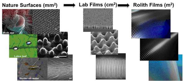
With the increased emphasis towards nanomanufacturing and commercialization of nanotechnology-enabled products, one key challenge is enhancing the innovation cycle. Through the innovation cycle, fundamental discoveries in the nanosciences are translated to applications and product scale-up. As many start-up or small company innovators are resource limited, the strategy of establishing strong partnerships with academic institutions and researchers provides a very effective path to extended R&D activities. Such partnerships typically lead to intellectual property, licensing, and technology transfer that enhance the cultures of academic researchers and small businesses alike, both in providing new perspectives for each into the innovation cycle, as well as accelerating the time and path to commercialization. A recent prime example of this scenario combines innovations emerging from collaborations between an academic institution and a small business start-up. An important aspect of this example is the technology that represents a nanomanufacturing platform targeting specific applications, with the ability to expand to future applications facilitated through the ongoing collaborative partnership. While this model is not new, the unique aspect is the rapid evolution towards industrial scale manufacturing platforms for nanotechnology-enabled products.

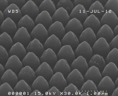
The partnership between Rolith Corporation and Professor Jay Guo’s Research Group at the University of Michigan has resulted in the licensing of a method to pattern nanoscale features in a surface over very large areas using a continuous optical lithography, very similar to semiconductor optical lithography, but using very different masks formed from a cylindrical polymer. Rolith CEO Boris Kobrin explains, “Our special design of the lithography tool and masks allows us to achieve a high resolution, not diffraction limited, high throughput and low cost. Our process is also not limited to semiconductor wafer form factor and is scalable to large surface areas, currently up to 1 meter long.” The Rolling Mask Lithography (RML) approach exposes a solid photoresist material to generate a pattern, therefore eliminating typical problems encountered with competing approach Nanoimprint Lithography (NIL), such as incomplete filling of mold features, demolding defects, residual layers, and so on. According to Kobrin, “being an optical lithography, RML can change a type of printed pattern from positive (for example, nanopillars) to negative (nanoholes) using the same mask just by changing the type of photoresist.” The RML approach is currently at the roll-to-plate (R2P) stage in which the patterns are generated from a continuous roll onto a flat surface. The approach is inherently scalable with the process being limited only by the width of the cylindrical mask, and optimization of the photoresist and light source. To date, Rolith has demonstrated scaling to 300mm x 1 m plates with throughputs between 0.5-1 square meter per minute. For feature sizes, Rolith has achieved 175 nm to date with targets of 50 nm in the coming year. In principle this technique can be transitioned to complete roll-to-roll (R2R) platforms for higher production throughput, which Rolith plans to do in the coming year.

“RML is a “platform” technology, which can be applied to a wide variety of applications and markets”, states Kobrin. “Our unique approach to nanopatterning, with its extraordinary flexibility and scalability, could open vast possibilities for advance products in commercial electronics, energy generation and storage, biotechnology, defense and others. Among applications on our near-term radar: AR surfaces, self-cleaning, anti-fog, anti-icing, anti-drag, anti-bacterial surfaces, transparent electrodes for displays, solar cells and LEDs, dye less color filters, absorption enhancement layers for solar cells, extraction enhancement layers for LEDs, 3D solar cells, and wire-grid polarizers.” Thus, such a platform technology provides an excellent example of nanomanufacturing technologies transitioning from academic research groups providing a platform to effective scaling the process for numerous high impact applications and markets.
