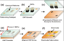
| With a relatively simple technique, Im and colleagues demonstrate the preparation of aligned single wall CNTs over large surface areas. |
Reviewed by Jeff Morse, Ph.D., National Nanomanufacturing Network

Im et. al. report a technique for direct printing of aligned CNT patterns onto glass substrates to form thin film organized CNT structures and devices. With this relatively simple technique, the authors demonstrate the preparation of aligned single wall CNTs over large surface areas. Vertically aligned CNT are first grown on a glass substrate by vacuum deposition and photolithographic patterning of catalyst seed layer films (Al 20 nm/Fe0.5 nm). Plasma chemical vapor deposition is then used to form patterned arrays of vertically aligned CNTs. The donor substrate with the patterned CNT arrays is then aligned face down with an acceptor glass substrate. The surfaces are brought into contact with approximately 5 kPa of downward pressure and slid 1mm in a constant direction. This printing process effectively transfers the CNTs to the acceptor substrate with the alignment in the direction of sliding, forming laterally aligned thick film CNT patterns. The authors report that the CNT films remain stable after transfer, thereby enabling subsequent process steps for further integration. For original vertically aligned patterns having a height of ˜10µm, printed CNT films 3µm thick were achieved. The authors further demonstrate the ability to create various patterns and line structures with this process, the linewidth of the printed films broadening slightly from the original patterns by only 5% for a 2 µm pattern.
In exploring the versatility of this method to control the thickness of the transferred film patterns, a subsequent sonication step was used to remove most of the film, leaving behind a monolayer thin film of aligned CNTs. Gold electrodes were patterned at either end of this monolayer film to form a field effect transistor (FET) device structure. Electrical testing exhibited high on/off ratio for the transistor, from which a hole mobility on the order of 10 cm2/V-sec was estimated. The aligned CNT films exhibited highly anisotropic electrical behavior. The authors also demonstrate an integrated gas sensor using a similarly fabricated structure.
While additional investigation must explore the range of subsequent process steps the aligned CNT films can withstand, as well as methods to further control the pattern fidelity and chemical properties of the deposited CNTs, the reported method offers a straight forward means for fabrication and characterization of integrated device structures. The ability to scale this process to wafer-level fabrication provides a versatile process approach commensurate with existing integrated circuit fabrication techniques. In addition, the ability to reuse the patterned catalyst layers for growth of vertically aligned CNT arrays follows green manufacturing approaches to improve the efficiency of materials utilization.
Image reproduced with permission from Im J, Lee IH, Lee BY, Kim B, Park J, Yu W, Kim UJ, Lee YH, Seong MJ, Lee EH, Yin YS, and Hong S. 2009. Direct Printing of Aligned Carbon Nanotube Patters for High Performance Thin Film Devices. Applied Physics Letters 94(053109). Copyright 2009 American Institute of Physics.
This work is licensed under a Creative Commons Attribution-NonCommercial-NoDerivs 3.0 Unported.
