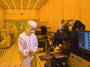
In this resource-conscious R&D environment, can you improve your company's chance of success by using a public Nanofabrication User Facility? How do you demonstrate the feasibility of an idea in a timely, cost-effective fashion? How do you leverage the manufacturing, processing and diagnostic tools that are available? For An Shyang Chu of PCB Piezotronics, an industrial user of the National Science foundation's (NSF) NanoTech User Facility at the University of Washington -- a member facility of the National Nanotechnology Infrastructure Network (NNIN) -- "having the right expectations and understanding of the tool set is the first step."
A recent workshop held at the ONAMI Micro/Nano Breakthrough Conference in Vancouver, WA, this September entitled "Nanotechnology User Facility and Nanomanufacturing Networks -- Models and Examples of Successful Interaction with Industry and Startup Companies" brought together leading experts and industry practitioners to discuss their research and development experiences with publicly accessible, U.S-based Nanofabrication User Facilities in both academic and national laboratories. (See our Facilities page.)
Research and commercialization of nanoscale technologies typically requires access to sophisticated fabrication and characterization equipment that is very expensive to acquire, operate and maintain. Such resources are normally beyond the reach of individual research laboratories and all but the largest companies. It is therefore a critical issue for progress in research, development, and commercialization of nanotechnology that shared facilities be operated according to business models which are consistently high in availability and technical performance, responsive to clients' needs, and financially sustainable.

This substantial investment by the federal government in Nanoscale Science and Technology User Facilities is further supported by a broad assortment of regional centers, laboratories, and consortia established in the areas of characterization, nanofabrication, and advanced materials.
Facility representatives -- including Francois Baneyx (NanoTech User Facility at the University of Washington), David Johnson (Center for Advanced Materials Characterization at the University of Oregon), and Michael Hjelmstad (Washington Technology Center Microfabrication Laboratory) -- provided overviews of facility capabilities, attributes, and technology focus.
Robert Hwang (Co-Director of the Center for Integrated Nanotechnologies (CINT) at Sandia National Laboratory), Robert Celotta (Director of NIST's Center for Nanoscale Science and Technology ), and Kenji Kitamura (Japan National Institute for Materials Science) discussed the range of unique science and technology projects at their facilities that provide the basis for collaborations with industry and academia.
Perhaps the most compelling portion of the workshop was the presentation of industrial user perspectives by Brian Ruby (Carbon Nanoprobes), Andreas Stonas (Voxtel, Inc.), and An Shyang Chu (PCB Piezotronics), representing small, medium, and large companies respectively. Each practitioner held their own unique view on issues such as intellectual property protection, collaboration with facility researchers, and subsequent transition of technology to manufacturing. Common themes among them were the needs to understand the capabilities of the User Facilities and to gauge expectation with respect to equipment performance, availability, and project goals. With appropriate foresight on these elements, interactions with industrial partners can be highly successful. The challenge remains, however, for both facility management and users to establish metrics for each specific project and interaction.
The workshop's concluding panel posed the following questions:
- What are typical barriers to successful feasibility demonstrations via the various Nanofabrication User Facilities?
- What resources and capabilities would be helpful in making the transition from demonstration to scaled production?
- Are new tools required that are not available or accessible presently?
The ensuing discussion was particularly enlightening regarding long-term goals and needs for technology transition. Industrial users cited foundry services as the next step for technology transfer; standardized equipment, materials, and processes supported by such services are a logical counterpart. Another key challenge would be to establish the necessary manufacturing scale-up and infrastructure for emerging processes and tools, a focus of the NSF's Nanomanufacturing-focused Nanoscale Science and Engineering Centers (NSECs).
The next step is to create a transitional roadmap to facilitate the insertion of new manufacturing methodologies into mainstream production, a daunting but necessary task to realize the potential of nanomanufacturing technologies of the future.
This work is licensed under a Creative Commons Attribution-NonCommercial-NoDerivs 3.0 Unported.
