
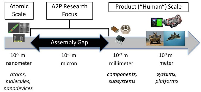
The benefits of nanotechnology and nanomanufacturing include significantly improved properties of many common materials when fabricated at nanoscale or molecular dimensions. Examples of these properties include quantized electrical characteristics, enhanced adhesion and surface properties, superior thermal, mechanical, and chemical properties, and tunable light absorption and scattering. Scaling these properties for nano-enabled products and systems, could offer potentially revolutionary performance and capabilities for defense, security, and commercial applications while providing significant societal and economic impact. Key challenges and barriers remain to realizing such nano-enabled technologies that are central to emerging nanomanufacturing techniques, including retaining the nanoscale properties in materials at larger scales, and the maturity of assembly techniques for structures between the nanoscale and 100 microns.
Recently, the Defense Advanced Research Project Agency (DARPA) has created the Atoms to Product (A2P) program to address and help overcome these challenges. The program seeks to develop enhanced technologies for assembling nanoscale elements coupled with integration and scale-up of these components into materials and systems to product scale in ways that preserve and exploit the distinctive nanoscale properties of the core element.
“We want to explore new ways of putting incredibly tiny things together, with the goal of developing new miniaturization and assembly methods that would work at scales 100,000 times smaller than current state-of-the-art technology,” said John Main, DARPA program manager, quoted from the DARPA website announcement. “If successful, A2P could help enable creation of entirely new classes of materials that exhibit nanoscale properties at all scales. It could lead to the ability to miniaturize materials, processes and devices that can’t be miniaturized with current technology, as well as build three-dimensional products and systems at much smaller sizes.”
The A2P program supports the emphasis on key challenges of nanomanufacturing for given applications extending previous investments in fundamental science and materials research. In this case, several emerging nanomanufacturing approaches and platforms are likely to contribute to such a program concept, including nanoimprint lithography, directed self-assembly (DSA), layer-by-layer (LBL) assembly, additive driven assembly, and hybrid processes incorporating solution-based and vacuum-based processing approaches. Further scalability through adaptation to existing manufacturing infrastructure such as roll-to-roll and print, additive manufacturing, or semiconductor “batch” type processing is likely to accelerate the pathway to commercialization, and further position these emerging nanomanufacturing processes for the eventual Factory of the Future.
To familiarize potential participants with the technical objectives of the A2P program, DARPA has scheduled identical Proposers Day webinars. Participants must register through the registration website: http://www.sa-meetings.com/A2PProposersDay.
The DARPA Special Notice announcing the Proposers’ Day webinars is available at http://go.usa.gov/mgKB. This announcement does not constitute a formal solicitation for proposals or abstracts and is issued solely for information and program planning purposes.
Image Source: DARPA