| Methods to fabricate 2D arrays of densely packed SWNTs remain an active area of nanomanufacturing research. In this review, a solution-based, post-process has been reported employing AC dielectrophoresis assembly of ultrahigh density SWNT arrays. The versatile approach has demonstrated the highest linear packing density of aligned SWNTs reported to date, with potential impact on the manufacturing of future nanoelectronics. |
Reviewed by Jeff Morse, Ph.D., National Nanomanufacturing Network
- Shekhar S, Stokes P, and Khondaker SI. 2011. Ultrahigh Density Alignment of Carbon Nanotube Arrays by Dielectrophoresis. ACS Nano Article ASAP 16 February 2011. doi: 10.1021/nn102305z.
Devices and processes exploiting the properties of carbon nanotubes (CNT) continue to experience notable progress towards applications including transistors, flexible electronics, displays, and sensors. While individual single walled nanotubes (SWNT) exhibit superior electronic transport properties for transistor applications, the ability to control chirality results in large device-to-device performance inhomogeneities. As a result approaches to fabricate CNT transistors have utilized random networks or multilayers of mostly semiconducting SWNTs. While these approaches have been shown to provide homogeneous device characteristics over large areas while enabling high current outputs, charge transport limitations are incurred due to tube-tube junctions within the conduction network. Ultimately such devices could benefit from perfectly aligned two-dimensional (2D) arrays of SWNTs, thereby exhibiting electronic properties approaching the intrinsic properties of the individual nanotubes. As a result, methods to fabricate 2D arrays of densely packed SWNTs remain an active area of nanomanufacturing research. One approach utilizes direct growth on substrates using a patterned catalyst. However, this approach, requires double growth techniques to achieve high densities, as well as high temperature (~900°C) growth and transfer printing steps to transfer the SWNT arrays to suitable device substrates. Ultimately a solution-based, post-growth assembly process would provide a more versatile, lower cost approach for device integration.

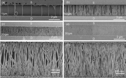
Recently, Shekhar et. al. reported on their investigation of AC dielectrophoresis (DEP) as a means to assemble SWNTs with ultrahigh density alignment. As a solution-based process, DEP has the advantage of enabling selected deposition of SWNTs onto prepatterned electrodes without the need for post-processing steps. The authors noted that to achieve effective high-density assembly and alignment, the SWNT suspension must be free of catalytic particles and contain mostly individual SWNTs, as the metallic catalyst particles could potentially migrate into the electrode gap and disrupt the SWNT assembly process. In their approach, the authors utilized a clean, surfactant free, aqueous SWNT suspension, employing the DEP approach to achieve ultrahigh density aligned SWNT arrays. The SWNTs had an average diameter of ~1.7 nm, and varied in length from 0.3-10 µm with a mean length of 1.5 µm as determined by scanning electron microscopy (SEM) and atomic force microscopy (AFM). The original solution contained a SWNT concentration of ~50 µg/mL, and was diluted using deionized water to achieve the desired concentration. Using prepatterned palladium electrodes with gap lengths of 2, 5, and 10 µm, and widths ranging from 25 µm to 1 mm, assembly was achieved by applying an AC voltage of 5 Vp-p at 300 kHz. The solution was applied by casting a 3 µL drop onto the substrate containing the electrodes and applying the AC voltage for 30 seconds which resulted in homogeneous assembly and better reproducibility. Reproducible control of linear array SWNT densities from 0.5 SWNT/µm to >30 SWNT/µm was achieved by variation of the nanotube concentration in the initial solution.

Thus, a solution-based, post-process has been reported employing AC DEP assembly of ultrahigh density SWNT arrays. The versatile approach has demonstrated the highest linear packing density of aligned SWNTs reported to date, with potential impact on the manufacturing of future nanoelectronics.
Images reproduced with permission from Shakar S, Stokes P, and Khondaker SI. 2011. doi: 10.1021/nn102305z. Copyright 2011 American Chemical Society.
This work is licensed under a Creative Commons Attribution-NonCommercial 3.0 Unported.
