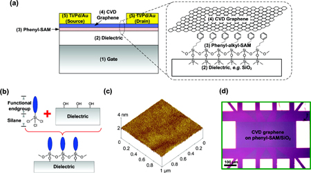
| As interest has grown in electronic devices and circuits fabricated from graphene thin films due to the large intrinsic carrier mobility, a key challenge remains to establish device integration strategies that enable field effect transistors (FETs) to have mobility approaching the intrinsic value. With thin film approaches to form graphene using chemical vapor deposition (CVD) on copper foils and subsequent transfer to silicon or other substrates for final integration, graphene has become a prime candidate for a range of applications in very large scale integrated (VLSI) circuits. Recently Liu et. al. have investigated the physics associated with the dielectric-graphene interface for integrated back gated FETs by controlling some of the detrimental scattering effects via application of self-assembled monolayers (SAM). Liu et. al. present a facile approach to improve the performance of scalable graphene transistors utilizing interfacial. The results provide valuable insights into the interfacial physics of graphene FETs. These results ultimately improve the potential application of graphene transistors towards VLSI circuits and applications. |
Reviewed by Jeff Morse, PhD, National Nanomanufacturing Network
- Liu Z, Bol AA, Haensch W. 2011. Large-Scale graphene transistors with enhanced performance and reliability based on interface engineering by phenylsilane self-assembled monolayers. Nano Letters. 2011; 11(2):523-528. doi:10.1021/nl1033842
As interest has grown in electronic devices and circuits fabricated from graphene thin films due to the large intrinsic carrier mobility, a key challenge remains to establish device integration strategies that enable field effect transistors (FETs) to have mobility approaching the intrinsic value. With thin film approaches to form graphene using chemical vapor deposition (CVD) on copper foils and subsequent transfer to silicon or other substrates for final integration, graphene has become a prime candidate for a range of applications in very large scale integrated (VLSI) circuits. Present FET integration approaches employ either bottom-gate designs utilizing a conductive silicon substrate, or a top-gate design. In either embodiment, carrier scattering effects at the dielectric-graphene interface have resulted in limited field effect mobility in comparison to the intrinsic carrier mobility of graphene. Additionally, the presence of mobile and immobile charge defects at the interface, interfacial roughness, and charge injection from the graphene to the dielectric under transient switching excursions result in unfavorable current-voltage (I-V) hysteresis characteristics that impact the reliability and stability of the integrated devices.

Electrical characterization of FET devices with and without the phenyl-SAM interface treatment exhibited a 150% improvement in extrinsic carrier mobility for the device with the SAM. Furthermore, the I-V characteristics exhibit no hysteresis during the process as the gate voltage is scanned from one polarity to the other, and remains very stable and uniform for devices fabricated over a relatively large area. The authors further analyzed the I-V characteristics for devices with and without the phenyl-SAM, applying models previously developed to predict the Dirac point shift during the voltage sweep. From this analysis the authors attributed the enhanced carrier mobility to reduced interfacial impurity and surface polar phonon scattering as well as the ultra-smooth SAM surface. The authors further found that the hysteresis present in devices without the interface treatment at room temperature was dominated by charge injection from the grahene to the graphene-dielectric interface. This finding was further supported by the Dirac point shift model results.
Thus a facile approach to improve the performance of scalable graphene transistors utilizing interfacial engineering has been reported. The results further provide valuable insights into the interfacial physics of graphene FETs. These results ultimately improve the potential application of graphene transistors towards VLSI circuits and applications.
Figure reprinted with permsision from Liu Z, Bol AA, Haensch W. 2011. Large-Scale graphene transistors with enhanced performance and reliability based on interface engineering by phenylsilane self-assembled monolayers. Nano Letters. 2011; 11(2):523-528. doi:10.1021/nl1033842. Copyright 2011 American Chemical Society.
This work is licensed under a Creative Commons Attribution-NonCommercial-ShareAlike 3.0 Unported.
