
While a significant amount of recent research and development has focused on flexible electronics and improvements in thin film transistor performance on flexible substrates, less attention has been given to electronics application requiring deformable layouts or extreme, complex surface shapes and curvatures. As flexible electronics technology matures, a growing number of applications require stretchable or extreme nonplanar systems approaches. Examples of these applications include electronic eye cameras, hemispherical or curvilinear electronics, prosthetic or medical sensors, and stretchable LEDs, displays, photovoltaics, sensors, or logic devices utilizing thin silicon. In all of these applications it is critical to maintain the performance of the active electronic devices as the substrate is deformed due to changes in shape or external applied forces. A key issue related to this is the adjustment in resistive properties of nanomaterial-elastomer composites as the elastomeric substrates is stretched, thereby necessitating different approaches for the design and manufacture of deformable electronic systems.
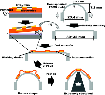
Characterization of the SnO2 NW FETs on the planar surface demonstrated excellent low-voltage switching characteristics and a nominal FET channel mobility of ~80 cm2/V-s. Because the regions where the FET devices were located were relatively large in comparison to the width of the metal interconnects between the devices, when the PDMS substrate was released and deformed to the original hemispherical shape, the majority of the stress was accommodated by the interconnects, which adopted arc-shaped geometries. This effect was modeled by the authors, which further confirmed that the electrodes remained within the elastic regime of mechanical behavior during deformation. Further characterization of the NW FET devices and interconnects under a range of deformations illustrated that while the shape and stress fields over the circuit elements and interconnects varied, the device performance was barely affected by the deformation conditions.
Thus, a facile approach to synthesize quality FET logic circuitry utilizing SnO2 NWs has been demonstrated. The authors further demonstrated that the circuits can be integrated on deformable flexible substrates where the design of interconnects can accommodate the stress fields resulting from a range of deformation conditions. The scaling of such a flexible electronics system design has implications towards a range of emerging applications.
Reviewed by Jeff Morse, PhD, National Nanomanufacturing Network
- Shin G, Bae MY, Lee HJ, Hong SK, Yoon CH, Zi G, Rogers JA, Ha JS. 2011. SnO2 nanowire logic devices on deformable nonplanar substrates. ACS Nano. 5(12): 10009-10016. http://dx.doi.org/10.1021/nn203790a
Figure reprinted with permission from Shin G, Bae MY, Lee HJ, Hong SK, Yoon CH, Zi G, Rogers JA, Ha JS. 2011. SnO2 nanowire logic devices on deformable nonplanar substrates. ACS Nano. 5(12): 10009-10016. http://dx.doi.org/10.1021/nn203790a. Copyright 2011 American Chemical Society.