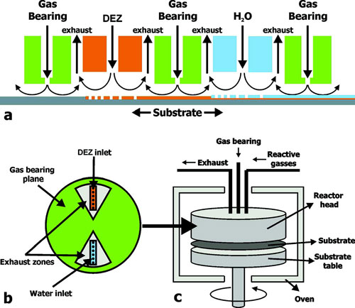
Atomic layer deposition (ALD) has emerged over the past decade as a viable alternative to physical and chemical vapor deposition (PVD, CVD) techniques for a range of strategic thin film coatings. This is due to the improved control of thin film properties including the incorporation of extrinsic dopants, reduction of contaminants, and the formation of intrinsic defects during film growth through a low temperature, non-vacuum process. These benefits result from the time-sequenced introduction of precursors in the deposition zone where selective and self-limiting half reactions occur on the surface. In this manner, thin-film growth is determined by surface kinetics, and is able to avoid parasitic gas-phase reactions. As such, film properties can be controlled by variation of temperature and reactant partial pressure. However, conventional time-sequenced ALD is not compatible with many scaled industrial applications as film growth rates (~0.01 nm/s) are rather slow due to the need to purge reactants during each growth half-cycle.

Investigating the electronic properties of the ZnO thin-films, it was further demonstrated that variations in reactant partial pressure could control the film stoichiometry, which in turn controlled the density of intrinsic defects. By controlling these parameters, the authors demonstrated the growth of 250 nm thick, n-type ZnO films with conductivity ranging from ¨~4-150 mΩ-cm with corresponding carrier mobility in the 10-30 cm2/V-s range. With associated optical transparency of ~85%, these ZnO thin films were suitable for a range of applications requiring transparent conductors or active transistors over large areas, for example photovoltaics and large area display backplanes. Thus a versatile materials growth technique has recently been scaled to a large area, high throughput process that is adaptable to a range of manufacturing platforms. Such a tool represents a disruptive manufacturing capability impacting both semiconductor and flexible electronics industries.
Reviewed by Jeff Morse, PhD, National Nanomanufacturing Network
- Illiberi A, Roozeboom F, Poodt P. 2011. Spatial atomic layer deposition of zinc oxide thin films. ACS Applied Materials & Interfaces. 4(1): 268-272. http://dx.doi.org/10.1021/am2013097
Figure reprinted with permission from Illiberi A, Roozeboom F, Poodt P. 2011. Spatial atomic layer deposition of zinc oxide thin films. ACS Applied Materials & Interfaces. 4(1): 268-272. Copyright 2011 American Chemical Society.
