The NNN recently caught up with Clint Landrock, Chief Technology Officer for Nanotech Security Corp., and one of the inventors of the recent patent, to get some further details regarding this exciting breakthrough.
NNN: I find the concept behind the recently issued patent US 8,253,536B2 intriguing. It seems this approach is a more active security feature, wherein a specific response is generated by an integrated circuit. Is this the first of its kind in the printed security and document authentication areas?
CL: Thank you, we certainly find the concept intriguing as well! Correct, this approach is for a more active security feature in that the unique structure allows the feature to appear to turn "on and off" as well as flash colors very brilliantly. However, it does not require an integrated circuit. Although visually the feature appears as though it is lit by an LED, it is the nanoscale structures that trap, intensify, and reflect ambient light.
We refer to this patent as our parent patent to which we have submitted a series of additional applications covering new uses and configurations stemming from this one. The patent marks the first for the use of nanoscale optical structures in security and authentication. The concept in general is a modular approach covering a series of embodiments.
This means we can utilize all or only certain technologies for security applications and manufacturing techniques. An example is using nano-structured optical arrays as a passive overt security feature where you can easily see the structure. Other examples include using the security feature to house critical encoded data that requires sophisticated equipment to detect.
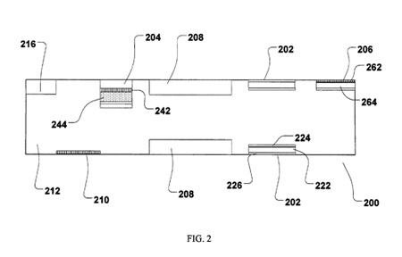
NNN: It seems there are two key components to the invention: first the printed optical features that enable both efficient optical transport and control of the image patterns printed in the documents, then the remainder of the active system that includes power source, electroluminescent device, and electronic circuitry that can provide a specific response to a given authentication query. Do you envision this entire system being utilized for every security application, or will some security applications only require specific elements?

NNN: This concept seems like it could be used for a range of possible markets, including games and interactive displays for consumer products. Do you see any opportunities for your technology there?
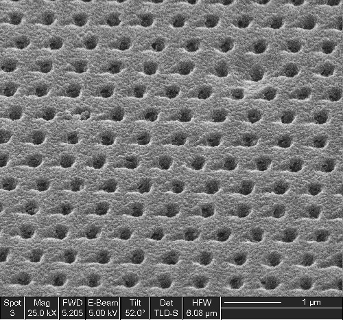
CL: Yes, we envision many applications and opportunities for our nanotechnology, for example, interactive displays on consumer products and specific light wave optical guides used in medical programs for sensing bacteria and diseases or for drug implementation. We arrange our optical nanostructures into microscopic arrays to create specific colors, including various shades of colors. These color arrays are similar to how LED displays create images but on a much smaller scale, and our technology could be used to implement brighter, higher resolution TV and computer displays in the future.
NNN: You mention that the printed optical patterns have utility for more efficient solar cells, and possibly other applications for displays where improvements in optical transmission of specific wavelength control are necessary. Are you targeting a market push in this area?
CL: We have several active R&D projects with our partners at Simon Fraser University developing applications for enhancing solar cells and electrical storage devices. Research and development is presently moving forward on active displays, windows, and various other optical filters. Our nano-optics were originally designed for improving solar panels, and this is something we are very interested to see come to market in the near future. By concentrating light into the solar panel using nano-structures on the surface, we can increase the efficiency without changing the solar panel and without increasing the cost.
Our manufacturing techniques for creating highly controlled nanostructures can be applied to batteries and super-capacitors by structuring their electrodes to maximize the surface area; more surface area equals more electrons, which means longer lasting batteries.
NNN: It seems many of the applications will involve high volume printing or roll to roll manufacturing platforms. Has Nanotech Security Corp. already demonstrated scaled manufacturing of this product?

NNN: Is there anything else you might elaborate on with respect to possible applications and competitive landscape for this technology?
CL: In terms of competitive landscape, we have seen some companies starting to work in this field but, to date, have not seen any direct competition in the nano space. This technology is in its infancy and we have first mover advantage after securing our parent patent. We have developed one of the first true engineered nanotechnologies that can be scaled effectively and produced using traditional manufacturing methods. Also, this is a true green technology that will not harm the environment, costs less to produce than current technology. and provides far improved security for authentication requirements. Our technology exhibits control of optical parameters (color, intensity, viewing angle, etc.) which allows us to expand into a diversity of applications from security authentication through medical into optical controls, which is unmatched.
In terms of market applications, in the security industry alone, this can be applied to authenticate not only banknotes, secure documents, and passports, but electronics, food and pharmaceuticals, and brand recognition. Each of these market segments represents billion dollar opportunities for Nanotech.
