Nanopatterning/Lithography
reproducible creation of a pattern [SOURCE: ISO/TS 80004-8 v1, 3.6]
- 3D lithography
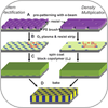
- Block copolymer lithography
- Block copolymer templating
- Colloidal crystal template lithography
- Deep ultraviolet (DUV) lithography
- Dip-pen nanolithography
- Electron-beam lithography
- Extreme ultraviolet (EUV) lithography
- Focused ion-beam (FIB) lithography
- Immersion optics
- Interference lithography
- Ion beam writing
- Ion projection lithography
- Micro-contact printing
- Microfluidic deposition
- Nano-imprint lithography (NIL)
- Nanoscale
- Natural lithography
- Optical lithography
- Phase-contrast photolithography
- Photolithography
- Plasmonic lithography
- Scanning force probe writing
- Scanning tunnelling microscope chemical vapour deposition (STM CVD)
- Soft Lithography
- X-ray lithography
NSF Center for Scalable and Integrated Nanomanufacturing
3112 Etcheverry Hall
MC 1740
Berkeley, CA
94720-1740
USA
The goal of the Center for Scalable and Integrated NAno Manufacturing (SINAM), an NSF Nanoscale Science and Engineering Center, is to establish a new manufacturing paradigm that integrates an array of new nano-manufacturing technologies. Founded in 2003, SINAM brings together an exceptional team of scientists and engineers from University of California Los Angeles, University of California Berkeley, Stanford University, University of California San Diego, University of North Carolina at Charlotte, and HP Labs.


