| Polymer bulk heterojunction materials offer a potentially low-cost, facile approach for the fabrication of efficient photovoltaic (PV) devices. He et.al. investigate the use of nanoimprint lithography (NIL) as a method to form patterned polymer blends generating a three-dimensional interpenetrating hierarchy of electron donor and acceptor materials. |
Reviewed by Jeff Morse, PhD., National Nanomanfuacturing Network
Polymer bulk heterojunction materials offer a potentially low-cost, facile approach for the fabrication of efficient photovoltaic (PV) devices. In order to optimize the efficiency of such materials systems, features must be synthesized balancing the tradeoffs associated with photon absorption, transport and charge separation of photogenerated excitons, and direct pathways for collection of electrons and holes. One approach to address these divergent design requirements is to devise an interpenetrating network of donor and acceptor materials having nanoscale features matching the typical exciton transport length on the order of 10 nm. Synthesis of these structures by spin-coating and annealing polymer blends leads to irreproducible morphologies, while phase segregation approaches generate interfacial regions that may trap exciton or charge carriers; both approaches impact exciton separation or charge transport and collection processes, and ultimately the overall efficiency of the device.
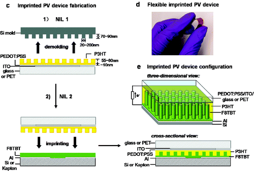
Recently He et. al. investigated the use of nanoimprint lithography (NIL) as a method to form patterned polymer blends generating a three-dimensional interpenetrating hierarchy of electron donor and acceptor materials. The authors utilized a master mold formed from silicon having a 75-80 nm deep dot pattern with feature sizes ranging from 25-200 nm. A film of electron donor polymer P3HT was spin coated onto a PEDOT/PSS coated ITO-glass substrate. The authors performed solvent assisted NIL at room temperature under nitrogen atmosphere to avoid degradation of the P3HT at elevated temperatures. The authors then annealed P3HT prior to demolding to improve the mechanical strength and crystallinity of the material. Similarly, a film of electron acceptor polymer F8TBT was spin coated onto an aluminum coated silicon wafer. The critical step in the process was to use the initially patterned film as the stamp in the subsequent imprint patterning of the electron acceptor film, thereby realizing a functional photovoltaic device architecture having precisely defined interface geometry. As such, interdigitated bilayer polymer structures were fabricated having features in the 25-200 nm range.

While these results are impressive considering that the authors used unoptimized polymer heterojunction materials, further expansion of this approach might explore enhanced photoabsorption of incident light using higher aspect ratio imprint patterns and investigate alternative materials to improve the exciton diffusion and carrier collection properties for the devices. The benefit of this method is that it can be adapted to virtually any polymer blends and materials.
Image reproduced with permission from He X, et al. Formation of Nanopatterned Polymer Blends in Photovoltaic Devices. Nano Letters Article ASAP 3 March 2010. DOI: 10.1021/nl904098m.Copright 2010 American Chemical Society.
This work is licensed under a Creative Commons Attribution-NonCommercial 3.0 Unported.
