Adhering to Moore’s Law of scaling of semiconductor devices and integrated circuits (ICs), the doubling of transistor packing density every eighteen months has lately become quite challenging for semiconductor manufacturers who need to address hard limits in lithographic feature resolution, increasing power dissipation per unit volume, and power utilization for mobile computing applications. As a result, new process and materials approaches are being included in semiconductor roadmaps in order to maintain this important trend, including the combination of top down and bottom up nanomanufacturing process steps, and lithographic approaches having ever-decreasing feature size and resolution. While some predictions of process approaches have included revolutionary methods incorporating bio-inspired nanostructures and processes to achieve templates with nanometer-scale critical features, it remains practical for the integrated circuit industry to maintain the process and tool infrastructure presently utilized. Therefore, acceptance of new methods and materials depends on a certain level of compatibility with existing fabrication lines. As such, the industry has been awaiting a major breakthrough that would propel technologies into the next millennium of advanced electronics and consumer products.

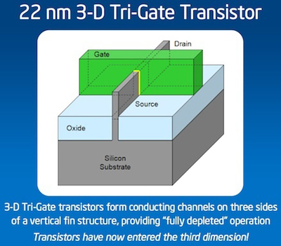
With the recent announcement by Intel regarding the development of the 3D trigate transistor, the breakthrough may just be upon us. The impact of 3D nanomanufacturing has been discussed previously with respect to the impact on performance of, for example, energy related technologies (solar photovoltaics, batteries, fuel cells) and data storage. With the Intel announcement, some simply remarkable fundamental improvements have been obtained which now promise to extend the adherence to Moore’s law for years to come. Most notably, the trigate 3D transistor design consumes only half the power, operates at lower voltages, and has an overall performance improvement of 37% in comparison to 2D planar devices fabricated with similar feature sizes. These improvements are extremely notable, particularly in light of Intel plans to fully implement this technology in manufacturing by year’s end, further transitioning from the present 32 nm lithography to 22 nm lithography lines. These breakthroughs highlight the impact of advanced nanomanufacturing on consumer products’ societal impact; this development will enable Intel to be more competitive in the mobile computing markets where power is critical, while further enhancing its line of personal computing products.
Since competition is stiff within the semiconductor industry, details of the 3D transistor integration process have not fully emerged; industry experts speculate that most companies have similar research and development activities, and that similar announcements will be forthcoming. These approaches will surely contribute towards the enhanced performance in consumer electronics for the foreseeable future as increased levels of integration and packaging are demonstrated. It will be quite interesting to determine the contribution of emerging nanomanufacturing methods with these new IC designs. Aside from advanced photolithography and coatings, prime examples of emerging nanomanufacturing processes relevant to the semiconductor industry include nanoimprint lithography, atomic layer deposition, and directed self-assembly. So while these approaches are not likely at the center of the recent breakthroughs in 3D transistors, they hold significant promise to extend the recent developments. One thing for sure, there are definitely some interesting times to come, and I, for one, will be closely following these developments and the impact they have upon the semiconductor industry and the broader nanomanufacturing community.
Finally, three events occurring over the coming months should be highlighted that provide technical presentations on developments in emerging nanomanufacturing research. These include the International Conference on Electron, Ion, and Photon Beam Technology and Nanofabrication, May 31-June 1, 2011 in Las Vegas, NV, the IEEE International Conference on Nanotechnology, August 15-18, 2011 in Portland, OR, and the Nanomanufacturing Summit 2011, September 25-27 in Boston, MA. These events provide a glimpse of the research trends that will impact future nanomanufacturing and nano-enabled products and commercialization.
This work is licensed under a Creative Commons Attribution-NonCommercial-ShareAlike 3.0 Unported.
