
ADDITIVE DRIVEN ASSEMBLY
An emerging nanomanufacturing technique referred to as additive-driven assembly enables block copolymer-nanoparticle (BCP-NP) solutions to be coated under certain conditions wherein the ordering and dispersion of the nanoparticles mimic that of the BCP morphology. By this approach, hybrid materials systems are assembled using strong interactions between the nanoparticle or nanoparticle ligand and at least one segment of the polymer. These interactions can be manipulated to drive organization of the structure, maintain excellent NP dispersion at high particle loadings and produce stable morphologies that resist aggregation. Ultimately, the specific ligands used to functionalize the NPs will dictate their position within the ordered BCP domains, which may be critical for a given device or materials application. An important advantage of this approach is the ability to create these structures at very high particle loadings. Finally, these systems can be prepared using solution-base processing, opening pathways for coating of the active layer of devices directly on a flexible substrate using roll-to-roll processing.
FLOATING GATE MEMORY DEVICE
Additive-driven assembly was used to fabricate a solution-based floating gate organic field effect transistor (OFET) memory device. A unique feature of OFET memory devices in comparison to a typical transistor device design is the inclusion of a metal or semiconductor charge-trapping layer located between a thin dielectric that enables charge tunneling from the semiconductor and a thick dielectric that blocks charge transport to the gate electrode. By incorporating NPs dispersed in a polymer dielectric as the charge-trapping elements, this approach has significant potential advantages for simplifying the fabrication process via a single solution-based coating step. To achieve high particle concentration in BCP matrix, the authors incorporated the use of NPs functionalized with short order ligands or organic additives that can hydrogen-bond to one segment of the BCP template. This strong, selective interaction actually drives the assembly of BCP systems, thereby inducing ordered morphologies in otherwise disordered systems. Utilizing this approach, CHM researchers were able to demonstrate unprecedented NP loadings in ordered BCP systems.
FLOATING GATE MEMORY DEVICE FABRICATION
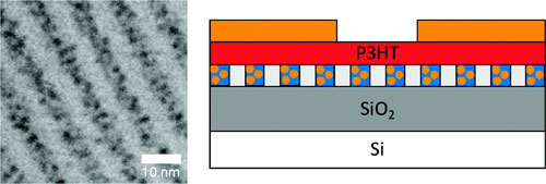
Gold NPs (~2 nm diameter) were functionalized with 4-hydroxythiophenol (Au-OH) and subsequently mixed with poly(styrene-b-2-vinyl pyridine) (PS-b-P2VP) blend at various NP concentrations. In this case, the 2-vinyl pyridine segments served as the hydrogen acceptor and the –OH ligands on the NPs acted as the donor in forming a selective, stable bond. The authors discovered that increasing the Au-OH NP loading in the BCP blend from 10 wt% to 30 wt% increased the segregation strength and ordering of the hybrid composite film, exhibiting a lamellar or grating-like morphology. For NP loadings >40 wt%, the resulting film indicated the onset of a transition between ordered morphologies. Comparing these results to unloaded BCP blends, as well as Au-OH NPs mixed with homopolymer blends, the authors observed no such ordering. Utilizing this strategy, the authors fabricated floating gate OFET memory devices using a highly doped silicon wafer as the gate electrode, with a layer of thermal silicon dioxide (SiO2) as the gate dielectrics. PS-b-P2VP films, with and without Au-OH NP loadings, were cast onto the SiO2 at a nominal thickness of 30 nm. A ~10 nm film of semiconducting polymer P3HT was formed on top of the PS-b-P2VP layer by contact printing, after which source and drain electrodes were formed by Au evaporation. The resulting gate width and length was 100 µm and 3 mm respectively.
FLOATING GATE MEMORY DEVICE TESTING
Electrical testing of the OFET memory devices exhibited excellent I-V transfer characteristics, with no observation of hysteresis during gate voltage sweeps for films without Au-OH NPs, indicating negligible charge-trapping sites in the bulk and gate dielectric interface. Device performance was studied for NP loading up to 60 wt%, with the observed shift in gate voltage corresponding to the NP loadings as the programming gate pulse voltage injects holes from the P3HT layer, which are then trapped by the NP layer. Thus, direct control of the memory window to practical levels is possible by variation of NP loadings in the hybrid BCP film. For NP loadings >40 wt%, the off current (Ioff) of the OFETs increased from 10-11 A to 10-7 A, indicating the presence of a conductive path in the charge-trapping layer as the NPs surpass the percolation threshold of the composite film. The memory devices further exhibited data retention over ten hours with read-out every 10 seconds.
CONCLUSIONS AND FUTURE WORK
This approach will enable the fabrication of well-ordered charge storage layers by solution processing and facile control of the memory windows by changing the density of Au NPs. The fabrication of large-area and high-density devices by using roll-to-roll printing techniques is now in progress. This extension requires use of a solution processable dielectric such as ZrO2 or ZrO2/polymer hybrid systems and patterning of the top and bottom electrodes to individually address storage clusters.
MORE INFORMATION
Prof. James Watkins, Director
Center for Hierarchical Manufacturing
University of Massachusetts Amherst
watkins@polysci.umass.edu
(413) 545-2569
www.umass.edu/chm
Summarized by the authors
- Wei Q, Lin Y, Anderson ER, Briseno AL, Gido SP, Watkins JJ. 2012. Additive-driven assembly of block copolymer-nanoparticle hybrid materials for solution processable floating gate memory. ACS Nano. http://dx.doi.org/10.1021/nn203847r
Figure reprinted with permission from Wei Q, Lin Y, Anderson ER, Briseno AL, Gido SP, Watkins JJ. 2012. Additive-driven assembly of block copolymer-nanoparticle hybrid materials for solution processable floating gate memory. ACS Nano. http://dx.doi.org/10.1021/nn203847r. Copyright 2011 American Chemical Society.