NSF Center for High-rate Nanomanufacturing, Northeastern University, University of Massachusetts Lowell

Impact
The directed assembly of polymer blends offers an advantage over block copolymers in that a wide array of polymers and molecular weights are readily available for use. For many practical applications, including nanolithography, the formation of features with complex and non-regular geometries is important, for example, square arrays, circle arrays, T-junctions, and 90˚ bends, which is easily accomplished using polymer blends. The direct assembly of polymer blends to achieve highly ordered uniform and non-uniform structures in short times provides a high rate, high volume approach to nanomanufacturing these structures. Alternatively, these patterned polymers can be used as flexible templates for the assembly of other nanodevices, etc., that are appropriately modified to “mate” with the patterned polymers.
Challenges, Issues, and Methods
- Patterning features having complex, irregular geometries
- Forming highly ordered uniform and nonuniform patterns in polymer blends on short timescales
- Directed assembly of multi-length scale patterns on functionalized surfaces


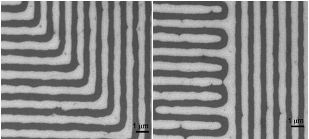
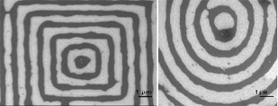
Figure 1: A set of generated non-uniform geometries by direct assembly of PS/PAA blends: a) 90Ú bends, b) T-junctions, c) square arrays, d) circle arrays. Dark areas are PAA and the light areas PS.
Progress
Chemically functionalized templates were prepared by patterning alkanethiols with different chemical functionality by combining electron beam lithography and self-assembly of alkanethiol molecules and then, using these chemically patterned templates to direct the assembly of polystyrene (PS)/polyacrylic acid (PAA) blends. The effect of specific chemical interactions on the ability to form these patterns in a rapid fashion was also investigated. Understanding this interaction provides the ability to control the site-specific deposition of polymer blends in very short times. The benefit of this approach is that the selective assembly process can be finished in 30 seconds and does not require the long annealing times (3-7 days) often required in the conventional assembly of block copolymers. It has been demonstrated that this method can be used to generate a variety of complex geometries including 90° bends, T-junctions, square and circle arrays, which have potential applications in fabrication of integrated circuits in nanoelectronics.

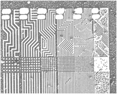
Figure 2: Images of the template directed assembly of polystyrene (PS) (dark)/polymethyl metacrylate (PMMA) (light) blends on chemically functionalized surfaces. Full view of the non-uniform geometry pattern from 300 nm down to 50 nm.
Industrial Sectors of Interest
Industry/market sectors impacted by the results of this test bed include lithography, electronics, semiconductors, and nanophotonics.
For more information, contact Prof. Joey Mead.
References
- Chiota J, Shearer J, Wei M, Barry C, and Mead J, Multiscale Directed Assembly of Polymer Blends Using Chemically Functionalized Nanoscale-Patterned Templates, Small 5 (24), pp. 2788-2791, 2009.
This work is licensed under a Creative Commons Attribution-NonCommercial 3.0 Unported.
