
| Graphene has attracted significant attention in recent years as a result of its high carrier mobility and saturation velocity, along with the ability to synthesize large-scale, high quality graphene sheets utilizing low-cost chemical vapor deposition (CVD) methods. Recently, Wu et.al. from IBM investigated the use of a diamond-like carbon (DLC) film grown on SiO2 as a substrate for transferring the graphene films. |
Reviewed by Jeff Morse, PhD, National Nanomanufacturing Network
- Wu Y, Lin Y, Bol AA, Jenkins KA, Xia F, Farmer DB, Zhu Y, Avouris P. 2011. High-frequency, Scaled Graphene Transistors on Diamond-like Carbon. Nature 472:74-78. doi:10.1038/nature09979
Graphene has attracted significant attention in recent years as a result of its high carrier mobility and saturation velocity, along with the ability to synthesize large-scale, high quality graphene sheets utilizing low-cost chemical vapor deposition (CVD) methods. Since graphene does not have a bandgap, a remaining drawback for transistor switching applications is the low On/Off ratio. While bandgap engineering techniques developed to address this issue have proven successful, challenges remain to create a sizable electronic bandgap without degrading the electronic transport properties of the material. In contrast, many radio frequency (RF) applications, such as amplifiers or mixers, do not require large On/Off ratios. In order to achieve their potential for commercialization, graphene transistor and integrated circuit designs for such high frequency applications must exploit low-cost, scalable graphene synthesis approaches. While high frequency RF transistors have been realized using exfoliated graphene or silicon carbide substrates, these approaches are not scalable. Transistors fabricated from graphene grown by CVD on copper (Cu) substrates then transferred to silicon dioxide (SiO2) substrates perform less favorably due to enhanced scattering by phonons and defects at the SiO2 surface.
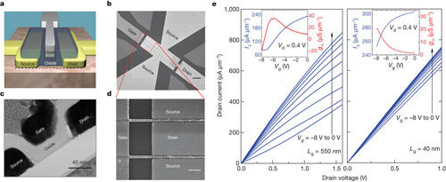
Measurement of transistor current-voltage (I-V) characteristics demonstrated excellent transconductance for drain voltages Vd=0-1.5 V and gate voltage Vg=0 to -8 V. The gate voltage modulation of the short gate length devices was much less than the longer gate devices, suggesting that contact resistance dominated the I-V characteristics. At this point, contact resistance for graphene transistors remains a key challenge. High frequency scattering parameters were used to measure the cut-off frequency (ft) of the devices, the frequency at which the current gain becomes unity. Transistors having gate length Lg=550 nm exhibited ft=26 GHz, whereas the devices having Lg=40 nm had ft=155 GHz. Most notably, the ft did not exhibit the typical inverse dependence on gate length (1/Lg) for the Lg=40 nm devices. Thus for the short gate length transistors, high-frequency characteristics are dominated by device contact resistance. Further optimization of RF design through minimizing gate capacitance and contact resistance, and increasing gate voltage modulation of the I-V characteristics will result in ultimate device performance.
Figure reprinted by permission from Macmillan Publishers Ltd: Wu Y, Lin Y, Bol AA, Jenkins KA, Xia F, Farmer DB, Zhu Y, Avouris P. 2011. High-frequency, Scaled Graphene Transistors on Diamond-like Carbon. Nature 472:74-78. doi:10.1038/nature09979