
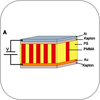
Thin films

Center for Atomically Thin Multifunctional Coatings

N340 Millennium Science Complex
University Park, PA 16802
A multidisciplinary and internationally leading center devoted to the design and development of advanced coatings based on two-dimensional (2D) layered materials.
Mission
To contribute to the nation’s research infrastructure base by developing long-term partnerships among industry, academia and government
To leverage NSF funds with industry to support graduate students performing industrially relevant research
Carnegie Mellon Nanofab

ECE Department
Pittsburgh, PA
15213
USA
A premier research laboratory in the College of Engineering, the Carnegie Mellon Nanofabrication Facility is one of the most well equipped university based facilities for thin film and nano/micro device development in the United States. The Nanofab includes a cleanroom with 2,600 square feet of class 100 space and 1,200 square feet of class 10 space, as well as three thin film labs.
The approach of transferring CNT thin films from one surface to another via a soft lithography technique suffers from limited ability to achieve good adhesion of the CNT films to the transferred substrate and imprecise alignment of the CNT patterns. A transfer technique that can be scaled to large area with high throughput processing at low temperature is being reported in this paper, demonstrating a scalable means to create aligned CNT thin film patterns on both rigid and flexible substrates.
The serial mechanical exfoliation method available can not be used for the assembly of graphene in the large scale. In this process, deposition of ultrathin few-layer (three to ten) graphene oxide, with parallel and controllable assembly, by dielectrophoresis between prefabricated electrodes has been demonstrated.

A perpendicular orientation of cylindrical microdomains in diblock copolymer thin films is achieved by control over polymer-surface interactions. The block which forms cylindrical microdomains is removed by UV exposure and a chemical rinse to yield a nanoporous polymer film. The porous film can be used as a template for electrodeposition of metal nanodots or as a mask for reactive ion etching.
An evaporation-induced flow in solvent cast block copolymer films can produce arrays of nanoscopic cylinders oriented normal to the surface and solvent annealing could markedly enhance the ordering of block copolymer microdomains in thin films. Without removing minor components, solvent-induced surface reconstruction can produce nanoporous structure in thin films. The porous film can be used as a template for deposition of quantum dots or as a mask for pattern transfer to the underneath substrates.
An applied electric field aligns a cylindrical-phase diblock copolymer perpendicular to a substrate. One polymer block is removed by UV exposure and a chemical rinse to yield a nanoporous polymer film. The porous film can be used as a template for electrodeposition of metal nanowires or as a mask for reactive ion etching.
KemLab

254 West Cummings Pk
Woburn, MA
01801
USA
Kemlab customizes electronic material formulations for the specific applications of customers.
We specialize in photoresist, ancillaries, and alternate coating technologies.
- Design new photoresist and ancillaries
- Modify commercially available photoresist
- Optimize film thickness, optical absorbance, photospeed, lithographic profiles, etc.
- Offer small volumes