Nanomanufacturing Processes
ensemble of activities to intentionally synthesize, generate or control nanomaterials (2.4), or fabrication steps in the nanoscale (2.7), for commercial purpose [SOURCE: ISO/TS 80004-1:2010, 2.12.]
Laboratory for Plasma Nanosynthesis100 Stellarator Road
Princeton, NJ, 08540
Laboratory for Plasma Nanosynthesis at Princeton Plasma Physics Laboratory (LPN-PPPL) combines PPPL expertise in plasma science with the materials science capabilities of Princeton University and other institutions. LPN-PPPL is conducting collaborative research on the fundamental physics of plasma synthesis of nanomaterials with the goals to understand, predict, and ultimately control the synthesis processes starting from the plasma generation to nucleation and growth of nanoparticles and nanostructures. The LPN-PPPL research program focuses on the integration of three areas:
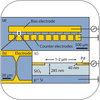
The approach of transferring CNT thin films from one surface to another via a soft lithography technique suffers from limited ability to achieve good adhesion of the CNT films to the transferred substrate and imprecise alignment of the CNT patterns. A transfer technique that can be scaled to large area with high throughput processing at low temperature is being reported in this paper, demonstrating a scalable means to create aligned CNT thin film patterns on both rigid and flexible substrates.
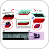
The serial mechanical exfoliation method available can not be used for the assembly of graphene in the large scale. In this process, deposition of ultrathin few-layer (three to ten) graphene oxide, with parallel and controllable assembly, by dielectrophoresis between prefabricated electrodes has been demonstrated.
Thin Film Electronics ASAHenrik Ibsensgate 100
Oslo, Norway
Thin Film Electronics ASA (“Thinfilm”) has 15 years of experience in the field of non-volatile memories using functional polymers. Thinfilm’s unique all-printed re-writable products are ideal for use in standalone consumer applications, including personalized toys and online-enabled games. They can also be integrated with logic elements, sensors, batteries, and displays for mass market applications such as all-printed RFID tags. The proven high volume roll-to-roll production of TFE’s printed memories provides the platform for its Memory Everywhere™ vision.
Guo Research GroupEECS Department
1301 Beal Ave.
Ann Arbor, MI
48109-2122
USA
Our lab is conducting research in the area of micro- and nanophotonics, organic solar cells, nanomanufacturing processes, and photonic-based ultrasound imaging technologies. Research Highlights:
* Roll to roll printed polymer organic solar cell based on a new ESSENCIAL technique;
* Multifunctional plasmonic color filters;
* High efficiency optoacoustic source based on CNT-PDMS composite;
* Ultra-high sensitivity polymer microring ultrasound detector;
* Spontaneous micropattern creation by localized wrinkling effect;
Pages